Printed Circuit Boards (PCBs) are an integral part of almost every electronic device. They are used to interconnect various electronic components and form the backbone of the entire system. With the increasing demand for high-speed and high-frequency applications, the design of PCBs has become more critical than ever. In such applications, signal integrity is of paramount importance, and one of the essential factors affecting signal integrity is impedance. This is where Bare Printed Circuit Boards with Impedance Control come into play.
What is Impedance Control?
Impedance is the measure of resistance to the flow of electrical signals through a circuit. It is the combined effect of resistance, capacitance, and inductance. The characteristic impedance of a transmission line determines how much of the signal is transmitted and how much is reflected. In high-speed and RF applications, signal reflections can lead to noise, distortion, and loss of signal integrity. Therefore, it is essential to design PCBs with impedance control to ensure that the signals are transmitted with a consistent and predictable impedance.
Bare Printed Circuit Boards with Impedance Control
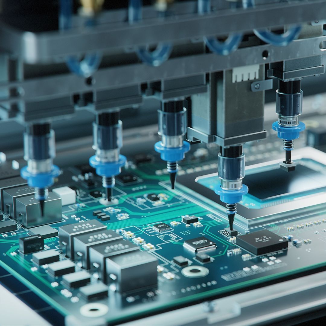
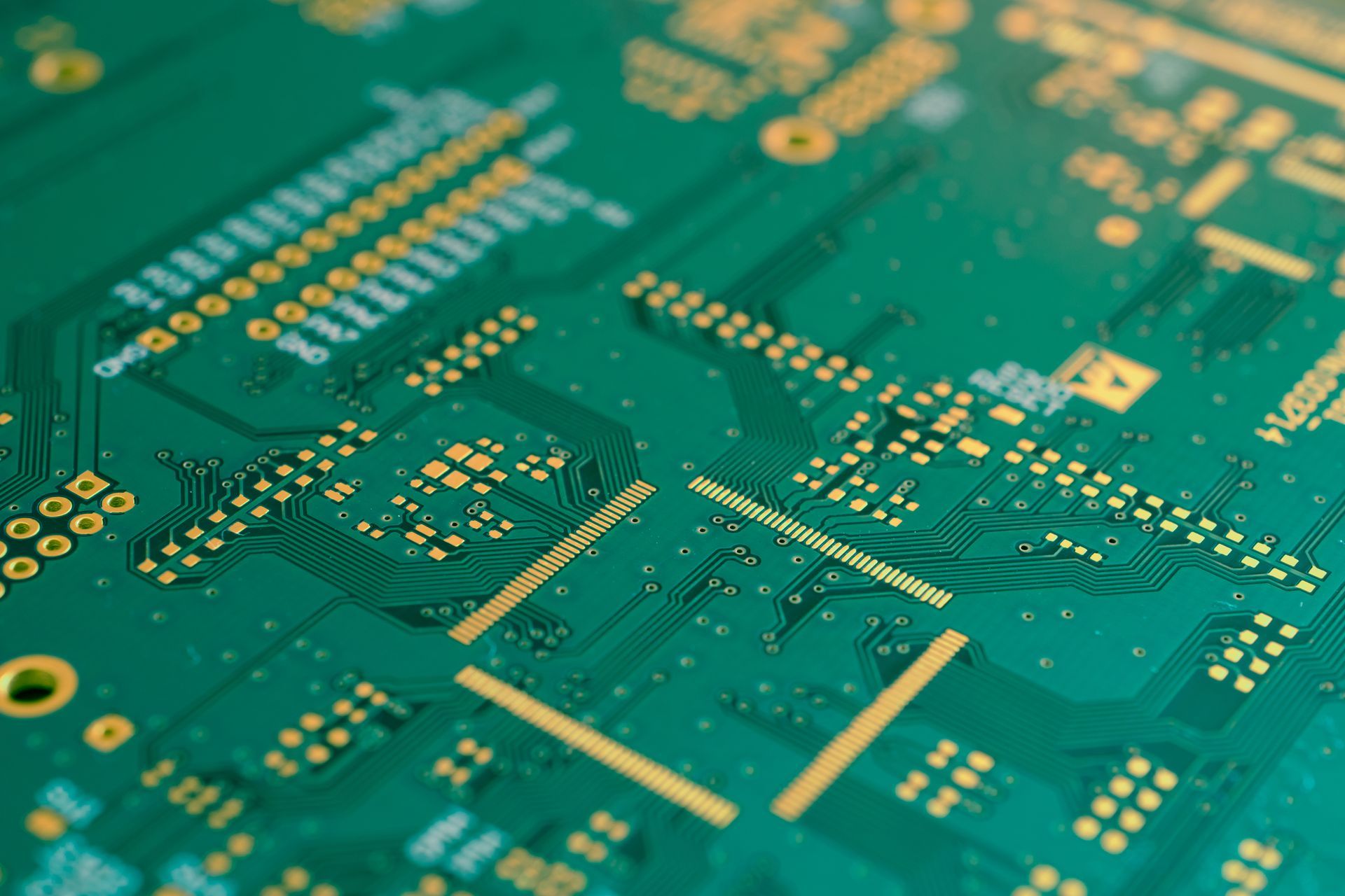
The fundamental components of any electronic system are bare PCBs. They are made up of a copper layer that is placed on a substrate material, which is generally FR-4. The necessary circuit layout is subsequently etched into the copper layer. Controlling the trace widths, spacing, and substrate material's dielectric constant results in the reduction of impedance. Utilising specialised software that can calculate the necessary values for impedance management, the PCB is designed.
Impedance control in bare PCBs is achieved by controlling the trace width and spacing. The trace width determines the amount of copper that is present in the circuit, and the spacing determines the amount of dielectric material between the traces. The dielectric constant of the substrate material determines the speed at which the signals propagate through the PCB. By controlling these parameters, the characteristic impedance of the transmission line can be maintained.
In high-speed and RF applications with operating frequencies between several megahertz and gigahertz, impedance regulation is crucial. In such applications, the signal rise and fall durations are brief, and the signal wavelength is about equivalent to the trace length. Due to the large transmission line effects that ensue, impedance regulation is essential to preserving the integrity of the signal.
Conclusion
High-speed and RF applications require bare printed circuit boards with impedance control as a critical component. These PCBs are designed using specialised software that can determine the necessary impedance control values. Controlling the trace width, spacing, and substrate material's dielectric constant results in the reduction of impedance. To maintain signal integrity, cut down on noise, and minimise signal reflections, impedance control makes sure that the signals are sent with a predictable and constant impedance. Impedance regulation is one of the most important aspects to pay attention to when designing RF and high-speed PCBs.
Here at M-Tek Assembly, we have years of industry experience, and our team of skilled engineers will guide you through the entire process. You will also be helping to save the environment by using M-Tek for bare-printed circuit board repairs. We have achieved a
net-zero carbon footprint by using electric vehicles, and for every circuit board we build, we plant a tree! Contact one of our SMT and PCB assembly experts today for assistance. Call
01189 455377 or follow us on
Twitter to learn more about our services.
Recent Posts