Our Objectives and Services
PCB Assembling UK
M-TEK Assembly: PCB Design, Prototyping and Assembly
What are Printed Circuit Boards (PCB)?
Printed Circuit Boards are fundamentally a board that connects electronic components. PCB assembly is the basic building block of any electronic design.
Over the year, PCB assembly has developed into a sophisticated and vital component in contract electronic manufacturing. At M-TEK, our team of electronics manufacturers specialise in PCB design, prototyping and PCB assembly. All while offering printed circuit board services including manufacturing and assembly are undertaken by experienced staff that have more than 20 years of experience in PCB designs for companies across the globe.
Let us help your business, no matter its industry, get your project up and running quickly! Enquire today and speak to one of our PCB assembling experts.
What is PCB Assembly?
PCB assembly is the process of soldering or attaching electronic components to a printed circuit board (PCB). The board itself is a piece of fibreglass or other substrates upon which copper tracks have been printed. PCB components are either surface-mounted or inserted into holes in the board and then the entire assembly is soldered.
These assembled PCB components are used in a wide variety of electronics. From computers and mobile phones to medical devices and military hardware; there are several advantages depending on the type and industry the printed circuit board is used in.
The main advantage of PCBs is that they allow for miniaturisation - ie, the ability to pack more components into a smaller space. This makes them ideal for use in portable devices and other high-density applications, such as for medical purposes.
Printed Circuit Boards
A printed circuit board (PCB) is an electronic circuit that is used in a device so it can provide a pathway to its electronic components and mechanical support. PCBs are used in a variety of devices, including laptops and computers, camera, mobile phone and tablets.
In the past, printed circuit boards were constructed through the tough process of point-to-point writing. Completing PCB this way typically led to various failures, including wire junctions and short circuits when wire insulation began to age and crack.
The Layers Of PCB
Did you know that PCB has multiple layers? These layers are:
What is the PCB process?
PCBs, or printed circuit boards, are the foundation of all significant electronics. Nearly every computational electronic gadget, including basic ones like digital clocks and calculators, incorporates these amazing inventions. Each PCB component has a specific function that is determined by the intricate system of copper pathways.
The printed circuit board process is a complex and detailed manufacturing process that starts with the design of the PCB.
Carbon Neutral PCB Assembly From MTek
PCB Design - Prototyping
Tested before PCB assembly begins
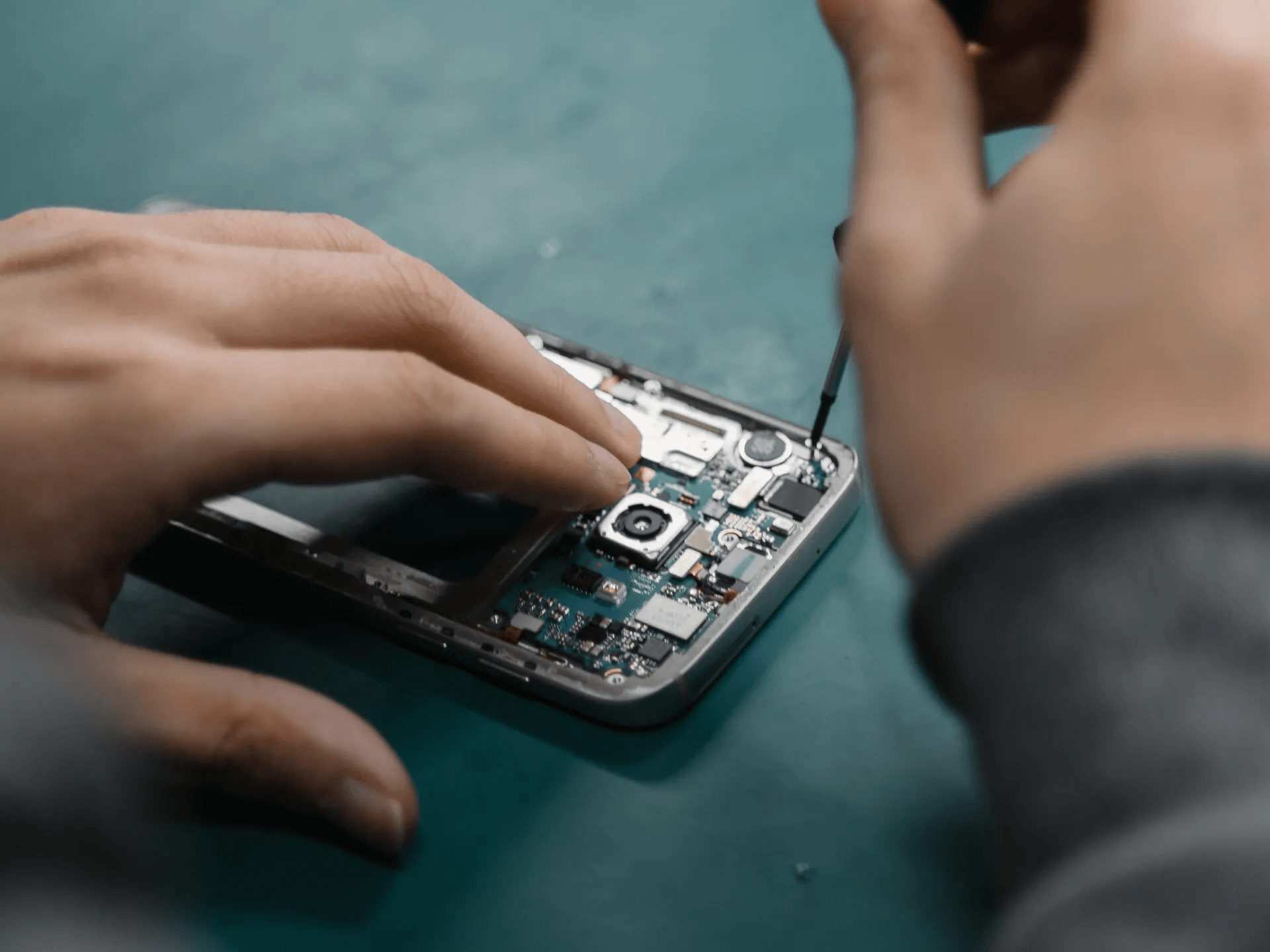
Our team of PCB electronics manufacturers take the design and creates a prototype. The prototype is sent to an assembler to place all of the electronic components on the printed circuit board.
After the PCB components are in place, it is then tested to make sure the printed circuit boards are working efficiently and effectively. If it does not, further changes will be made and a second prototype created.
Once the board is functional, an actual production board is created and will feature all of the PCB components.
When prototyping has been completed, it is time for PCB assembly to begin. The final step in this process is to install all of the PCB components into your enclosure or housing for use with their intended purpose.
PCB Assembly - Installation
Into enclosure or housing
Our team of electronics manufacturers will place the thin, stainless steel stencil over the printed circuit board. We will apply solder paste evenly across the circuit board. Then, the surface mount technology components are placed on a PCB and soldered onto the circuit board surface. The solder paste needs time to solidify and remain in place to reflow.
After the surface mount technology components are soldered into place, PCB assembling inspection needs to be undergone. This includes manual checks from our contract electronic manufacturing experts, automatic optical inspections, using an AOI machine and high-powered cameras. We also use X-RAY inspections to ensure a more complex inspection of the printed circuit boards. For more information on our services, click here.
The plated-through-hole (PTH) components need to then be plated through the printed circuit board, by either manually or wave soldering. Once this is complete, our specialists will complete final inspections, product support and simulate tests for the PCB assembly.
PCB - Final Product
Final product ready to be used.
The PCB assembly technician will work with your design and install all of the necessary parts on the board. Once it has been built and tested by our experienced specialists, at M-Tek Assembly, we'll ship it right to you!
With high-quality products and a low price, our PCB assemblies can help you to stay competitive in your industry and increase your overall efficiency.
As a complex and detailed process in the contract electronic manufacturing industry, it is important that every stage is efficiently completed. That’s where M-TEK Assembly is here to help. We have years of experience in PCB assembly. So, if you have any questions,
please contact us here.
Our Turnkey Services
M-TEK also offers PCB turnkey services to help you from start to finish with everything that's required for the successful completion of your PCB project. Our team of PCB assembly technicians have years of experience in the industry and our team of skilled engineers will help you every step of the way.
We can provide engineering assistance, testing setups & equipment, prototyping, programming software development, product support and much more.
With high-quality products and a low price, our printed circuit board turnkey services can help you to stay competitive in your industry and increase your overall efficiency.
Contact us today to get started on your project!
Why Use PCB Assembly?
There are a number of reasons why you might choose to use PCB Assembly over other methods of assembling contract electronic manufacturing components.
Why M-TEK Assembly?
M-Tek Assembly is a PCB manufacturer that offers high-quality PCB assemblies at a low price. We have years of experience in the contract electronic manufacturing industry and our team of skilled engineers will help you every step of the way.
Our team of PCB assembly technicians can provide engineering assistance, product testing setups & equipment, prototyping, programming software development, MRP software and much more. With high-quality products and a low price, our PCB assemblies can help you to stay competitive in your industry and increase your overall efficiency.
Contact us today to get started on your project!
Carbon Neutral PCB Assembly
Here at M-TEK, our experienced PCB assembly technicians are proud to announce that we now offer carbon-neutral PCB assembly. What does this mean for you and your company? It means that all of our PCB assemblies are now certified carbon-neutral.
We achieve this by offsetting the carbon emissions from our manufacturing process with renewable energy credits by partnering with Carbon Footprint. For every printed circuit board we build, we plant a tree in Uganda.
This is just one more way that we're working to be environmentally responsible and help you reduce your carbon footprint.


