When it comes to PCB assembly, testing a design is a crucial aspect of the process. To ensure that a PCB is fit for purpose there are multiple techniques which can be implemented to ensure there are no errors with the design. Flying Probe testing is one of the most widely used test techniques. We will cover everything you need to know about flying probe testing in this article from what it is to how it works. But first, let’s learn the history behind it.
What is In-Circuit Testing?
In the past, in-circuit testing was originally developed for examining PCB assemblies.
ICT, or in-circuit testing, is a potent instrument that examines each component separately to find problematic ones. ICT provides a "schematic verification" and is a very accurate testing method. The ICT, a fully automated test, assists in finding flaws in an assembly so that they can be fixed before it is finalised. ICT is typically done in two stages, such as power-on and power-off tests. As the name suggests, tests are run in the first half of Power-off Tests before power is applied, and tests are run in the second portion after power is applied.
What is Flying Probe Testing?
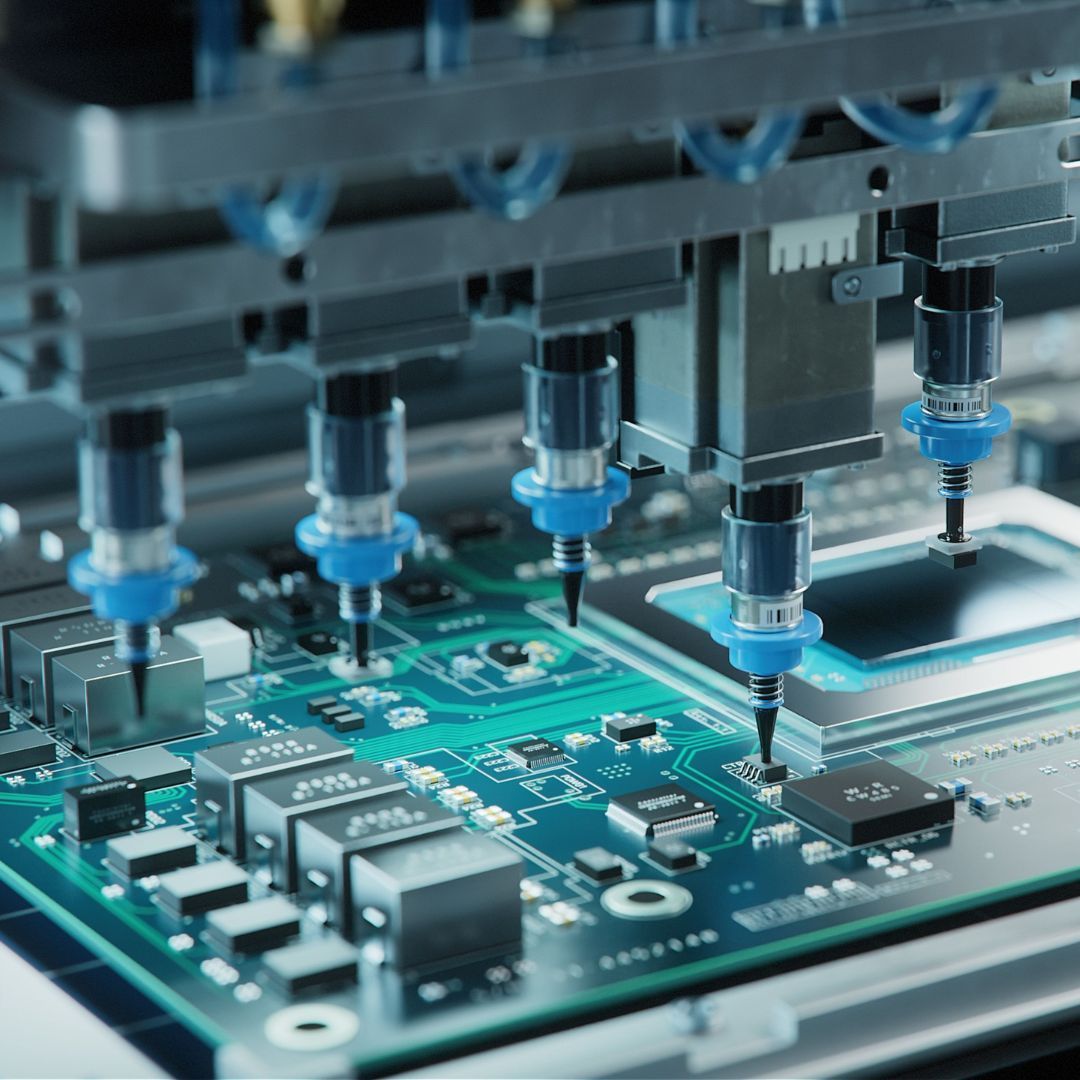
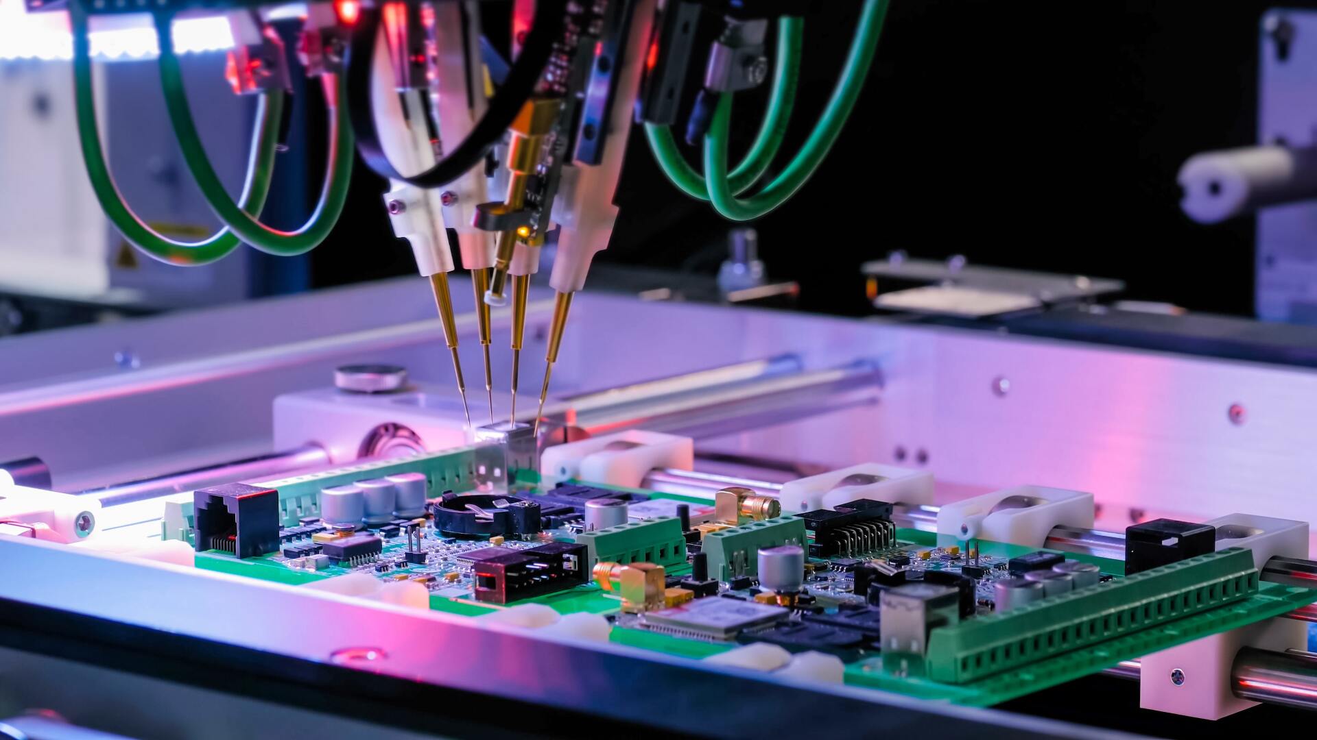
The Flying Probe Test (FPT), to put it simply, is an automated device with a few probes that concurrently "fly" over the top and bottom of a PCB to make contact with the test spots. A flying test probe is moved from one test point to the next in line with the software setup for the particular board being tested.
Electrical tests are carried out using high-precision needles on FPT machines to ascertain the condition of a PCB (component). These tests are a cost-effective method in the early stages of development and low-to-medium volume production because they don't require the use of specialised tools.
How Does Flying Probe Testing Work?
Flying probe testing is typically favoured for low-volume PCB assembly and prototype circuit board testing since it is simple and less costly for these smaller quantities. The biggest benefit is the speed, since tests may be developed and made accessible in a matter of days or hours, depending on the complexity of the circuit board, even for higher volumes.
Below, we go over how it works in a few steps:
- Programming an FPT Test: The complete circuit board is to be tested using this design. Typically, an offline PC is used for this task along with an FTP test programme generator tool. Typically, this calls for ECAD files, BOMs, and Gerbers. To declare the values of the components being tested, test points, component formats, offset, debugging, etc. on the machine itself using a Masterboard and complete the design of the test programme.
- Uploading the Program to the FTP Tester: Inside the FTP tester, the circuit board assembly that needs testing is put on a conveyor belt and moved to the location where the probe is carried out.
- Using Electrical and Power Test Signals: Following the completion of these tests on the probe locations, the measurements are read. This procedure will determine whether a particular PCB component achieves the desired outcomes (component). Any flaw in the unit, which results in a failed test, will be indicated by any failure or departure from the defined programmes and expectations.
How Can M-Tek Assembly Help?
Since 1996, at
M-TEK, we have continuously delivered high-quality printed circuit boards and other electronic manufacturing services to a variety of industries. We employ various cost-effective and time-saving methods, including box-build assembly and flying probe testing. Get in touch with one of our experts for help with your SMT and PCB assembly today. Call us on 01189 455377, or follow us on
Twitter to stay up to date with our services.
Recent Posts