Follow Us
How is a printed circuit board made?
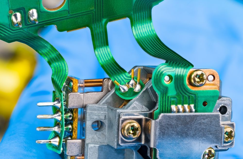
Printed circuit boards (PCBs) are a plastic board that is designed to connect electronic components. PCBs are commonly used in electrical products from computers to hairdryers. Every circuit board is unique to its design requirements, but how are they made?
Designing a Printed Circuit Board
The first aspect of the PCB assembly process is the design of the board. Like any manufactured product, a circuit board requires a base plan for its overall design. Depending on your desired requirements for the circuit board, our PCB designers can create a suitable design for the board using industry design software. After the design process has been completed, checks will be made to ensure the data meets the required standards of the manufacturer.
Preparing a Printed Circuit Board
The primary base of a printed circuit board is often laminate, due to it being ideal for use with copper. The material of the laminate is a strong body for the PCB and the copper can be pre-bonded on both sides. In the preparation, stage hygiene is of utmost importance to prevent dust from making contact with the board. To ensure the printed circuit board is dust-free, it is passed through decontamination and is prepared with a layer of the photoresist film.
The PCB is then exposed to UV light which passes through the clear sections of the board to harden them to ensure they are not conductive. After the PCB has been exposed to UV, the board is then washed with an alkaline solution to remove any unhardened film. The PCB is dried after this and a final check is done to ensure no defects have occurred during the process.
Etching
The etching part of the process is done to eliminate any unwanted copper that remains on the PCB. The most common way to remove copper from a printed circuit board is through the use of a strong chemical. The chemical is used to remove any unwanted copper to leave you with only the wanted protected copper.
Drilling
The drilling aspect of the PCB assembly process involves preparing the components for attachment to the PCB by drilling accurate holes into the board. A computer is used to drill the holes as they need to be small and precise, the computer is used to control the movement of the drill to provide accuracy. Computers are often used to save time in high production.
Plating
The PCB copper connections cannot be soldered on their outer layers. During the plating process to ensure that the copper connections are suitable to be soldered, the surface of the circuit board is plated with tin, nickel or even gold. A masking material is also used to protect the areas of the board which should not be soldered. The masking material is often a type of polymer coating to prevent short-circuiting.
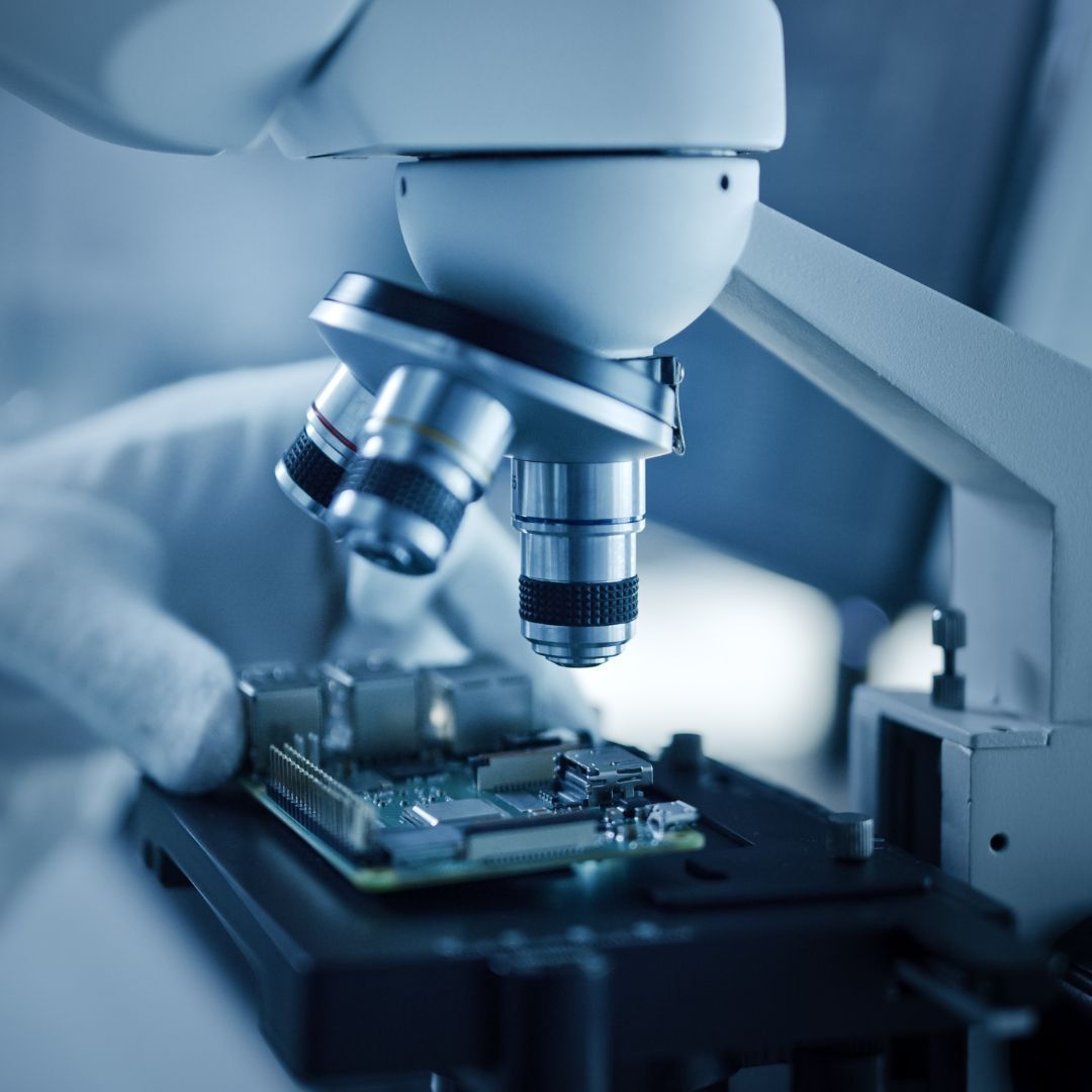
Testing
After plating a quality check is done by a technician on the printed circuit board. The quality tests often include the use of a computer program to supply a small amount of voltage to each conductive point on the board. This is to ensure that the PCB is functioning as intended.
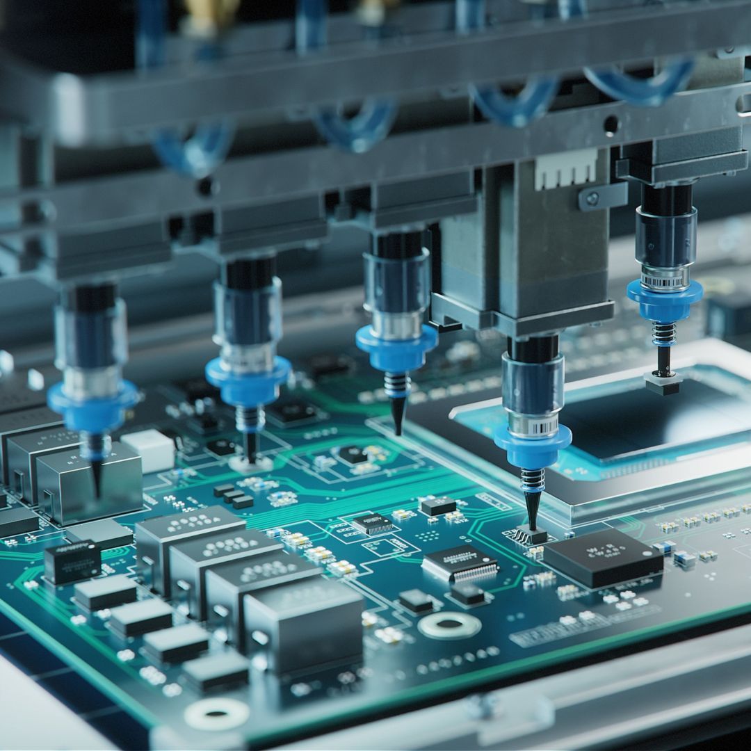
PCB Assembly
The final part of the PCB assembly process involves the assembly of all the different electronic components onto the appropriate part of the circuit board. Various techniques can be used to achieve this including surface mount assembly and through-hole assembly. These techniques both use soldering to ensure that every component is fixed securely to the printed circuit board.
At M-Tek Assembly, we are a PCB manufacturer that offers high-quality printed circuit boards assembly at a low price. We have years of experience in the industry and our team of skilled engineers will help you every step of the way. By choosing M-Tek for your printed circuit board repairs, you will also be doing your part to save the planet. We have achieved a net-zero carbon footprint from our use of electric vehicles, and for every circuit board we build, we plant a tree! Get in touch with one of our experts for help with your SMT and PCB assembly today. Call us on 01189 455377, or follow us on Twitter to stay up to date with our services.
Recent Posts
Share This Post
Leave A Comment
Call Our Team
Want to find out more about our PCB assembly services? Speak to our team to find out how we can help you.

M-Tek Assembly. A Specialist Full Turnkey Electronic Manufacturing Partner. Full Procurement, Assembly, X-RAY, Programming & Test Services
