As a business owner, your time is valuable, you should design your printed circuit board (PCB) properly from the beginning. We cover everything you need to know in our comprehensive guide, including PCB design fundamentals and stages, materials and structure, and more, so you're ready to design the strongest printed circuit board feasible. In this article, we will discuss the process of PCB design and where to look if you want to outsource your PCB assembly.
What is a PCB?
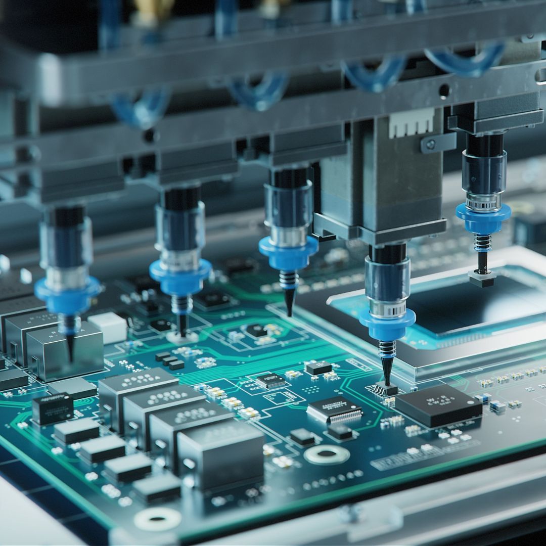
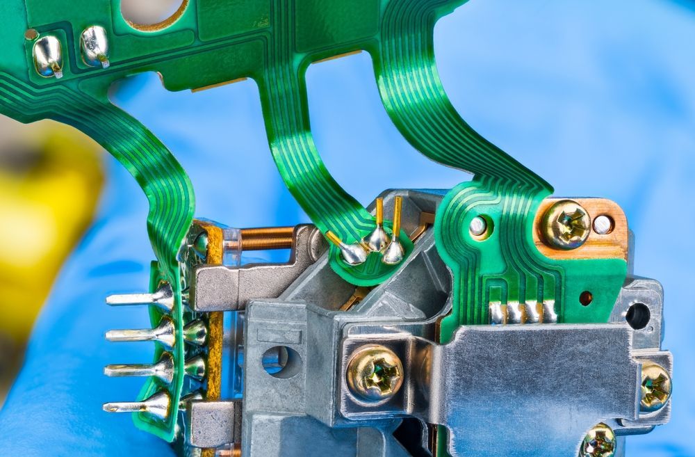
A PCB is a flat surface or base of insulating materials that consists of a pattern of conductive materials and components. Printed circuit boards are the foundation on which all other electronic components are assembled, whether they are simple single-layered boards used in your garage door, a six-layer board in your smartwatch, or a 60-layer, very high density and high-speed circuit board used in supercomputers and servers. However, all PCBs must begin somewhere, and that somewhere is with design.
Why then are PCB design fundamentals so essential? Numerous extensive revisions can significantly delay the completion of a project, likely to cost you time and money. Working with PCB engineering experts from the start is essential for designing for manufacture and assembly and ensuring a final, cost-effective product that works efficiently and effectively.
PCB Design Guide
Here are the nine steps to designing a printed circuit board, from initial drawings to final files:
Electrical Parameters
Before beginning a PCB design, you should be familiar with and understand the system's electrical parameters, which include:
- Current maximums
- Voltages
- Types of signals
- Capacitance restrictions
- Characteristics of impedance
- Considerations for shielding
- Circuit component and connector type and location
- Detailed net wire diagram and listing
Developing the schematic
One of the first steps is always to create a schematic, which refers to the design of the board's purpose and function at the electrical level. It is not yet a mechanical representation at this point.
To create your PCB layout, use a schematic capture tool.
The correct PCB provider will collaborate with principal engineers to create a schematic that includes a software platform. This demonstrates how your PCB will function and where the parts will be placed. After you finish your schematic, the engineer will load it and see how it fits in the intended device.
Create your PCB Stack Up.
Because impedance refers to how much and how quickly electricity can travel down a trace, this is important to consider early in the PCB design stage. The stack up influences how the mechanical engineer designs and fits the PCB into the device.
Establish design guidelines and specifications.
This step is largely governed by IPC standards and acceptability criteria, the industry group for PCB and electronics manufacturing. These specifications cover everything you need to know about PCB manufacturing. Find a PCB layout provider who is well-versed in IPC standards; this will prevent you from getting major revisions and production delays.
Set up your components.
When it comes to component placement, the customer and PCB provider will often discuss design and layout guidelines. There may be standards stating that certain components should not be situated near others just because they affect electrical noise in the circuit. Every component (in most cases, connectors) will have data sheets provided by the PCB provider, which will then be placed in the structural layout and sent to the client for approval.
Make drill holes.
The elements and a connection drive this step. Approximately half of the flex circuit designs on the market are double-sided, which means they connect to the drill hole on the bottom layer.
Trace the traces.
After you've placed the components and drilled the holes, you're ready to route the traces, which means connecting path segments.
Labels and identifiers should be added.
Add any labels, identifying information, markers, or reference designators to the layout now. Reference designators are useful for indicating where specific components will be placed on the printed circuit board.
Make design/layout files.
This is the last stage of the layout process. This file includes all of the data about your printed circuit board, and once produced, your PCB is ready for assembly.
About M-Tek Assembly Ltd
M-Tek Assembly is a PCB manufacturer that provides low-cost high-quality printed circuit board assembly. We have years of industry experience, and our team of skilled engineers will assist you every step of the way. By using M-Tek for printed circuit board repairs, you will also be helping to save the environment. We have achieved a net-zero carbon footprint through the use of electric vehicles, and we plant a tree for every circuit board we build! Contact one of our experts today for assistance with your SMT and PCB assembly. To learn more about our services, call 01189 455377 or follow us on Twitter.
Recent Posts