PCB X-Ray Inspection: What You Need to Know!
With micro components and details to care for, maintaining the quality of printed circuit boards (PCB) is becoming increasingly difficult for PCB manufacturers. We apply various PCB inspection techniques to rectify errors in your PCBs to ensure they work efficiently. X-ray inspection, also referred to as Automated X-ray Inspection (AXI), is one of the more popular techniques for rectifying errors.
What is PCB X-Ray Inspection?
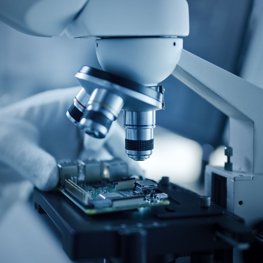
As the name would suggest, PCB inspection involves using an x-ray. By inspecting the printed circuit board with an X-ray, you can detect any defects that may cause issues going ahead. Inspections by x-ray allow for a better inspection of PCBs compared to other methods such as optical and thermal imaging.
What Defects can You Pick Up on with X-Ray Inspections?
So, where can you implement the use of PCB x-ray techniques? Our x-ray inspection process is to detect the following defects in PCBs.
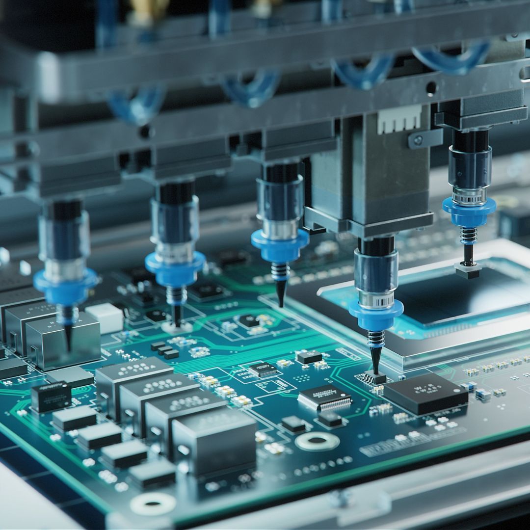
Area packages like CSPs, QFNs and chips are used in a variety of different industries including broadcast and telecommunications. These packages contain several solder joints, which may result in hidden complications due to invisible defects, also known as soldering defects. This is one of the many reasons why at M-Tek Assembly Ltd, we employ AXI to detect the following defects: solder bridges, solder voids, insufficient soldering, open circuits and many more.
With the demand for compact PCB packages on the rise, so are the defects in components. Packages contain minuscule components that offer excellent performance and save energy. Often meaning these components, when faulty, may raise complications when defected. Our AXI can be used to detect lifted lead, missing and misplaced components if this occurs.
Our x-ray inspection techniques can also be used to detect issues with BGA and CSPs, helping to find hidden defects such as BGA shorts and BGA open circuit connections. The x-ray inspection process has become an essential part of the PCB manufacturing process.
Why Choose M-Tek Assembly Ltd
Here at M-Tek Assembly Ltd, we are proud to announce that we are now certified carbon neutral. For every circuit board we build, we plant a tree in Uganda. We are working hard to be environmentally responsible and help you reduce your carbon footprint by working with us.
With M-Tek, we believe the customer always comes first! That is why we pride ourselves on our commitment to existing and new customers alike with our rapid responses and continue to expand our excellent quality services into new sectors and industries.
To learn more about what we do or if you need a PCB x-ray inspection, get in touch with a member of the M-Tek team today by calling 01189 455 377 or following us on
Twitter.
Recent Posts