What is a Reasonable PCB Design For an RF Circuit?
The advancement of communication technology has seen an increase in the number of wireless radio frequency (RF) circuit applications, such as in mobile phones and Bluetooth products, and the RF circuit has been the core technology of radio propagation. Nevertheless, in recent years, the gradual adoption of 4G and obvious increase in data transmission order of magnitude have posed challenges to RF circuit PCB design. And besides, the number of signals transmitted by an RF circuit increases hundreds of times per day.
In this article, our M-Tek Assembly experts will present a reasonable PCB design for an RF circuit, with features such as small volume and obvious anti-interference abilities.
Substrate Material Selection
Because some ICs (integrated circuits) are implemented on the substrate, a suitable substrate for RF circuits must first be selected as a blueprint carrying electronic components. In words of substrate material selection, the first elements to consider are dielectric constant, dielectric loss, and coefficient of thermal expansion, of which dielectric constant is the most important because it greatly affects the impedance and transmission speed of the circuit, especially those circuits with extremely high frequency that have strict dielectric constant requirements. As a result, it is generally recommended to select substrate material with a low dielectric constant.
Printed Circuit Board Design Procedure
The first step in PCB design is to create a schematic diagram, which must be completed using computers. The schematic diagram design is carried out using PCB design software, which includes all electronic analogue components. First and foremost, a circuit diagram is created by replicating the real circuit in a computer. The circuit diagram must then be linked to the corresponding components. Following that, an operation simulation is carried out based on the schematic diagram to test the possibility of the basic operation.
The pattern and size of the PCB can be scientifically determined after the schematic diagram is designed. The pattern and size of the PCB can be optimised following the position, dimension, pattern, and other parameters to ensure that the entire system performs optimally. The positions of location holes, view eyes, and reference holes must be determined during this process.
Find all of the necessary components. Ordinary components are easily accessible in a warehouse. If components are not available in the warehouse, they must be procured or manufactured. The final step is to detect circuit operation to ensure that the performance of the circuit can meet the requirement and that the circuit is essentially stable.
Component Design
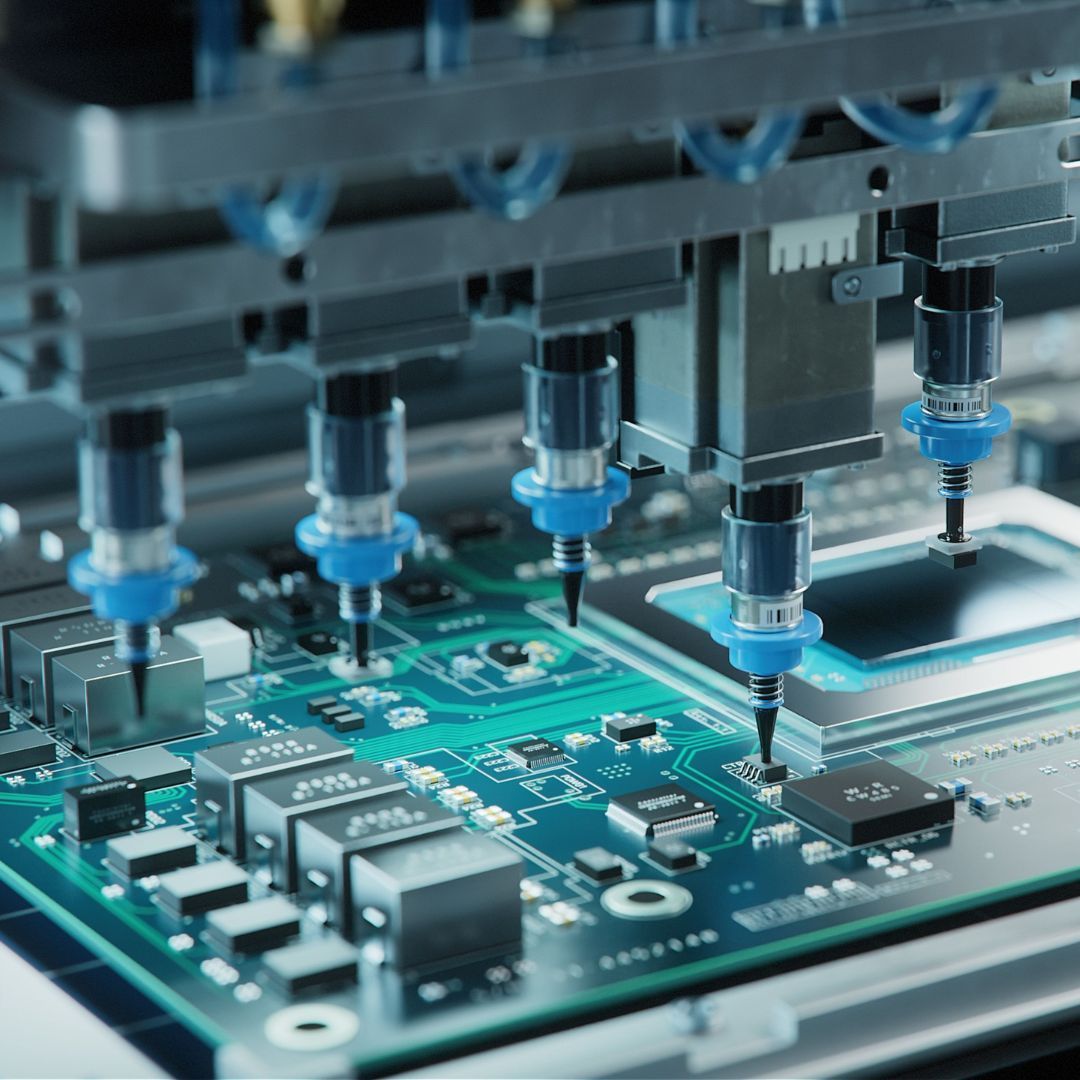
In contrast to standard component layout, all components in an RF circuit are so small due to the small scale of the circuit that SMT (surface mount technology) is used for component layout and an infrared reflow oven is used for soldering microelectronic components. Soldering is an important connection in RF circuit design, and its quality has a direct impact on the overall quality of the circuit. Excellent electromagnetic compatibility between electronic components is required for the PCB of an RF circuit, which is the most important factor to consider.
Because electromagnetic radiation between different electrical parts impacts the independent operation of each electronic component, it is essential to select anti-interference components.
Routing
Routing follows a basic layout and is divided into detailed routing and overall routing. The former relates to the routing of the circuit's various modules. Even though detailed routing occurs in IC design, preliminary detailed routing is carried out before component procurement. Sometimes only minor changes are required.
Overall routing denotes mutual routing between modules or network routing between power and each module. Some factors must be considered during the overall routing process. As a result of position specificity and varying distances between modules, numerous constraints will be imposed. If each module is treated as a point and the connections between them are determined, the best plan with the shortest routing length will be generated to save material costs and make the circuit look simple and tidy.
You will also be helping to save the environment by choosing M-Tek Assembly Ltd for your
PCB assembly. We have achieved a net-zero carbon footprint by using electric vehicles, and for every circuit board we build, we plant a tree! Contact one of our SMT and PCB assembly experts today for assistance. Call us at 01189 455377 or follow us on
Twitter to stay up to date on our services.
Recent Posts