What You Should Consider Before PCB Designs
The design process of printed circuit boards (PCBs) is crucial. Without proper PCB designs, the final product may be short-lived and experience a handful of problems associated with electromagnetic interference, board failure and result in added repairment costs.
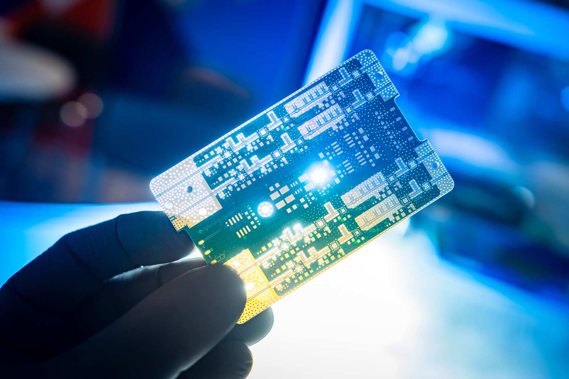
Considerations must be taken into account during the PCB designs and layout process. Here at M-TEK, we have over 20 years of experience in the electronic manufacturing industry and understand the importance of correctly laying out any printed circuit boards. Find out more about the considerations needed to be taken before PCB designs here.
Basic Constraints
The first step to make is to fully understand the board’s constraints. For this, it is important to know the complete size and shape of the board, to ensure that there is adequate room for all the components needed.
Ensure that you are aware of the functionality of the board and what components are required to determine the size of PCB designs. This should be the most important stage and will determine the rest of the steps of PCB designs and their layout. In addition, the number of layers should also be considered before components are placed. Additional layers will increase the cost, however, it will improve the board’s efficiency and the ability to include more tracks.
Placement of Electric Components
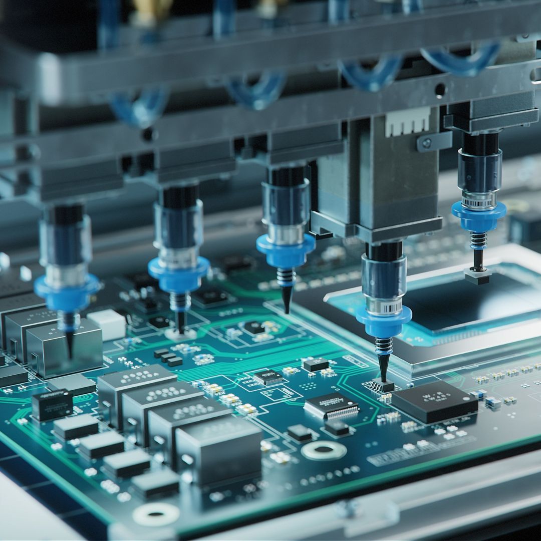
Though it may seem easy enough, thought should be taken when placing the various components in the PCB designs stage. Even though selecting your components is difficult, mounting them on the circuit board adds a whole new degree of complexity.
The issue is that while you want to place as little space as possible between components, you soon have problems with resistance, overheating, traces, and technological limitations. Finding the right balance between functional parts and space savings is important and should be considered before PCB designs. Also, care should be taken to not place components on the solder side of the PCB which will sit directly behind the plated through parts.
Overheating
A major concern with printed circuit boards is that they can easily overheat. This is because electricity passes through the PCB and, in the case of bad PCB designs, can result in permanent damage.
Through PCB designs, you should consider component distance and leave room for heat venting methods as well.
Prototyping
Making your PCB designs with meticulous planning and blueprinting is the best method to solve these issues. The blueprint will only take you so far; ultimately, you'll need to spend money on a real prototype PCB to test your concepts. Fortunately, you may work with makers of printed circuit boards for prototypes to develop a smaller version of your PCB before making a larger version.
At M-TEK Assembly, all our printed circuit boards are designed and manufactured with the client’s best interest in mind. We have various capabilities to ensure that thought is put into our PCB designs and that includes rapid prototyping and testing and programming before shipping. For more information, click here.
Placement Order For PCB Designs
The arrangement of components on the board is one of the most basic PCB design principles. Connectors should come first, followed by power circuits, precision circuits, crucial circuits, and then the remaining components.
There are several factors that affect the circuit’s routing priority, including power output, noise susceptibility, generation, and routing capacity. So it is important to ensure these elements are placed in the correct order and that there are spaces in between parts.
Here at
M-TEK, we understand the importance printed circuit boards can have in a variety of industries. When it comes to PCB designs, you should have the confidence that each electrical component runs efficiently for your business.
Contact one of our SMT and PCB assembly experts today for assistance. Call us at 01189 455377 or
follow us on Twitter to stay up to date on our services.
Recent Posts