A Comparison of Traditional vs. 3D Prototyping for PCBs
The world of electronics is ever-evolving, and with that, the need for better and more efficient ways to prototype PCBs (Printed Circuit Boards) has become increasingly important.
In the past, traditional prototyping methods were the norm, but in recent years, 3D printing technology has emerged as a viable option. In this article, we'll compare traditional vs.
3D prototyping for PCBs, looking at their benefits and drawbacks.
What is Traditional Prototyping?
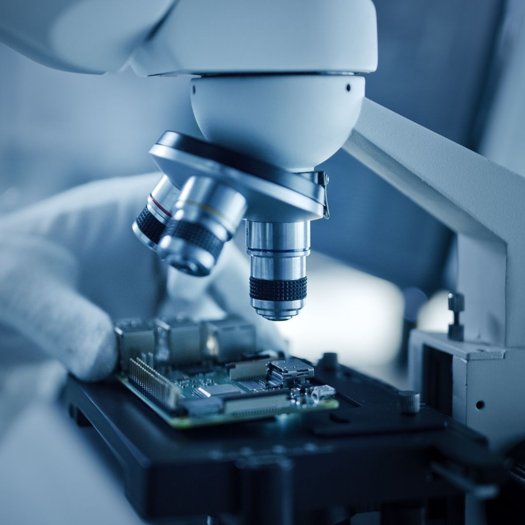
Traditional PCB prototyping is a method where a PCB is created by applying a layer of copper to a substrate, which is usually made of fibreglass or a similar material. This process is known as the copper etching method. The copper is then selectively removed using a chemical process, leaving behind the desired circuit pattern.
Advantages of Traditional Prototyping
One of the main advantages of traditional prototyping is that it's a
well-established method that has been around for a long time. The process is tried and tested, and as such, there is a wealth of information available on how to create PCBs using this method.
Another advantage of traditional prototyping is that it's
relatively inexpensive. The materials required for traditional prototyping are widely available, and the equipment needed is relatively cheap compared to 3D printing technology.
However, traditional prototyping also has its drawbacks. For example, it can be time-consuming and requires a lot of manual labour, especially during the etching process. Additionally, traditional prototyping doesn't always produce the most accurate PCBs, and the process can be quite messy.
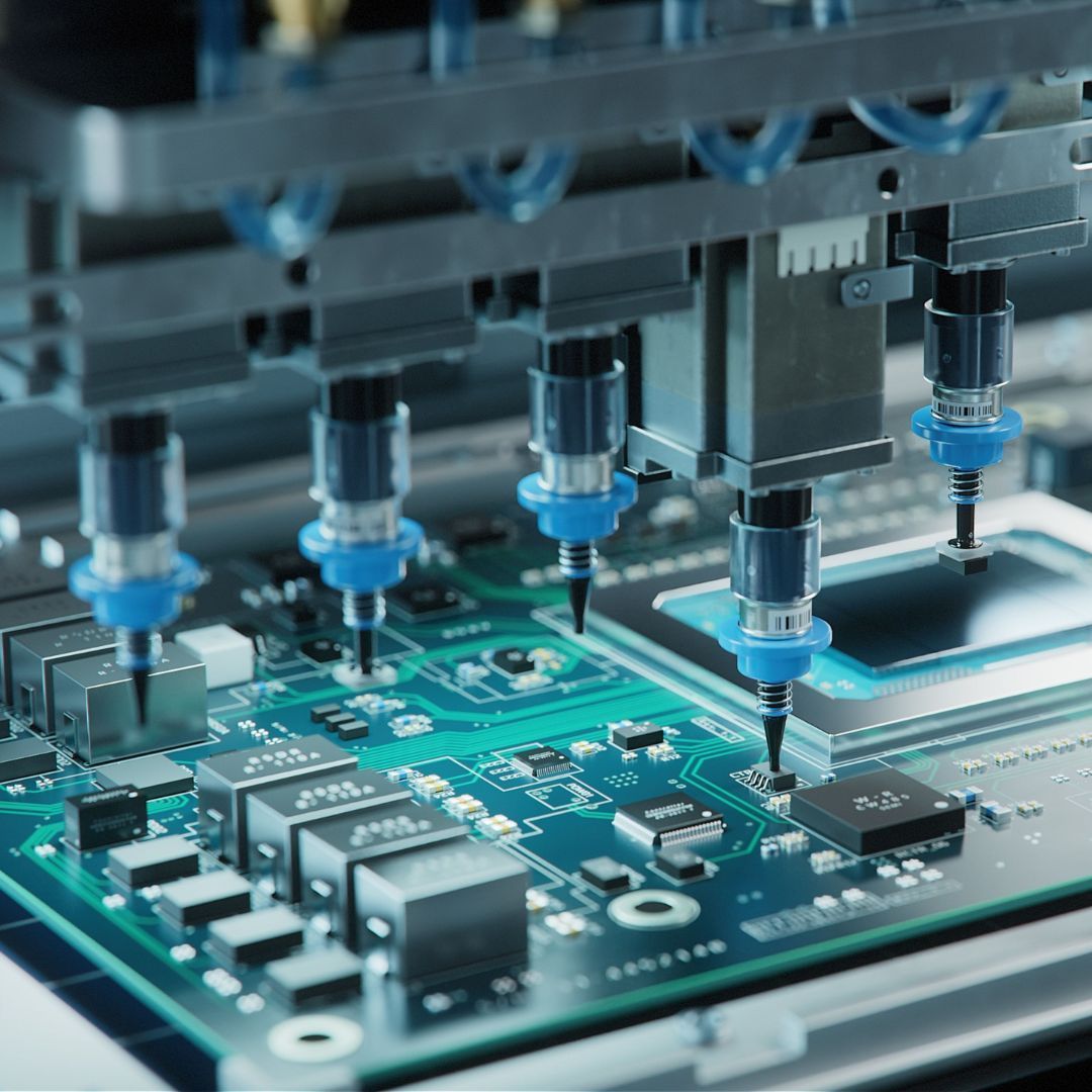
3D Prototyping
3D printing technology has made significant strides in recent years and has become a viable option for PCB prototyping. With 3D printing, a PCB can be created layer by layer, with each layer being printed onto a substrate using a printer.
3D Prototyping Advantages
One of the main advantages of 3D prototyping is that it's very accurate. 3D printing technology allows for very precise and detailed designs, resulting in very accurate PCBs. Additionally, 3D printing technology is much faster than traditional prototyping, and as such, can produce PCBs in a shorter amount of time.
Another advantage of 3D prototyping is that it's
much cleaner than traditional prototyping. The printing process is enclosed, and as such, there is no mess to clean up afterwards.
Comparison
When it comes to choosing between traditional vs. 3D prototyping for PCBs, there are several factors to consider. One of the most significant factors is the level of accuracy required for the PCB. If the design requires a high level of accuracy, then 3D prototyping is likely the best option. However, if the design is less complex, then traditional prototyping may be more appropriate.
Another factor to consider is the cost. Traditional prototyping is generally less expensive than 3D prototyping, but this is not always the case. The cost of materials and equipment can vary depending on the specific project.
Finally, the level of experience and expertise required is also an important consideration. Traditional prototyping is a well-established method, and as such, there is a wealth of information available on how to do it correctly. However, 3D prototyping is a newer technology, and as such, there is a learning curve involved. Additionally, 3D prototyping requires some technical knowledge, which may not be necessary for traditional prototyping.
M-Tek Assembly
We at M-Tek Assembly have decades of experience in the field, and our group of knowledgeable staff will help you every step of the way. We have achieved a net-zero carbon footprint by using EVs, and for every PCB we build, we plant a tree!
Contact one of our SMT and PCB assembly experts today for assistance. Call 01189 455377 or follow us on Twitter to learn more about our services, including vacuum casting.
Recent Posts