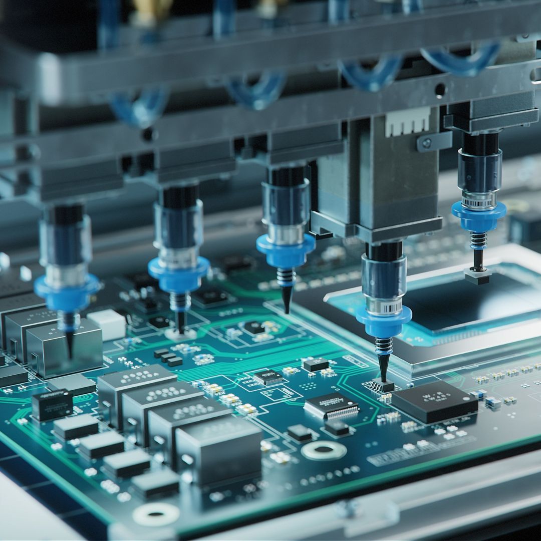
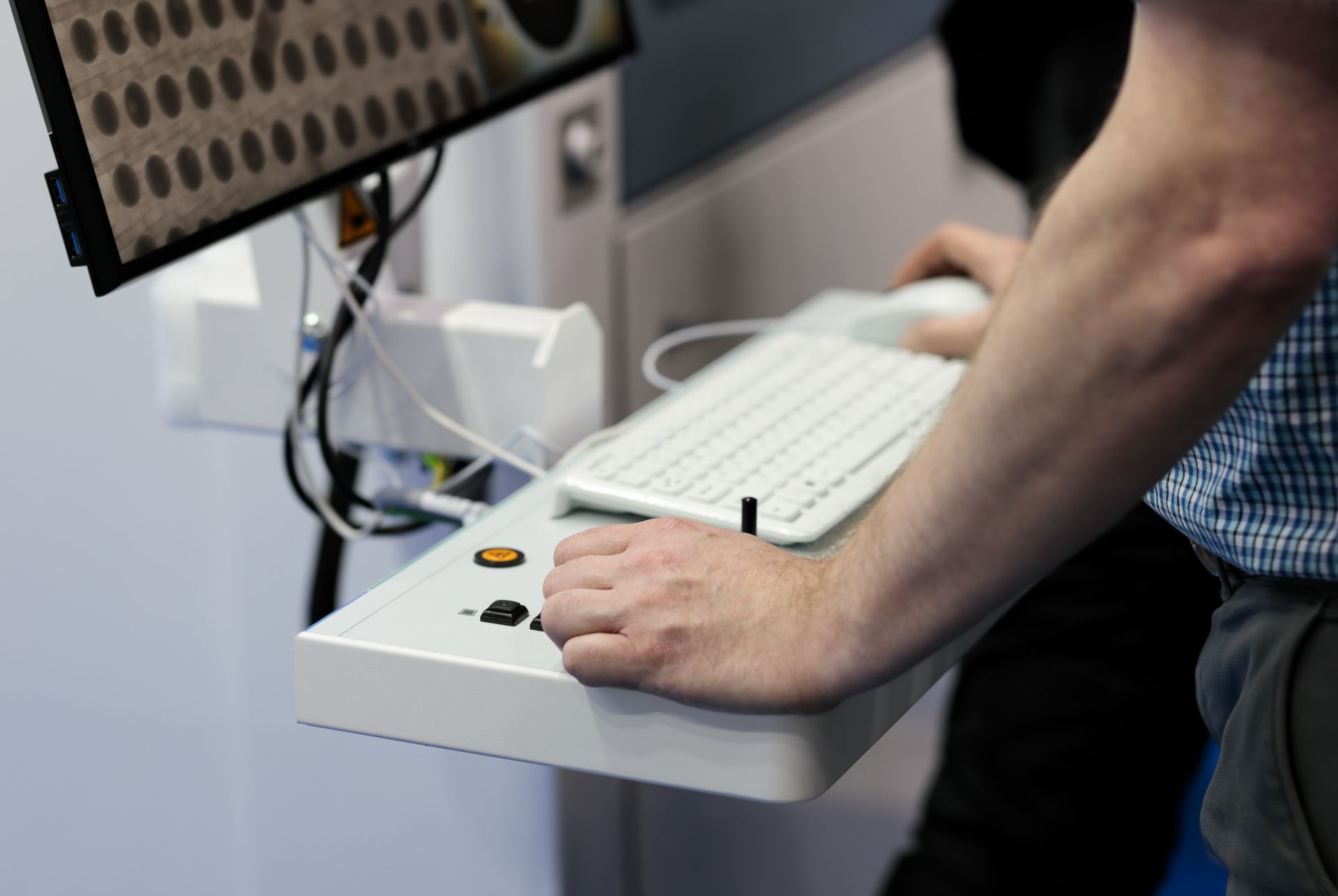
Sub-micron X-ray inspection is a critical tool for quality control and reliability assessment in the manufacturing of modern electronics. It enables engineers and technicians to inspect the internal structure and composition of electronic devices at the sub-micron scale, which is crucial for detecting and preventing defects and ensuring product reliability.
In the field of electronics, the trend is towards miniaturisation and increased functionality. This requires devices to be smaller, lighter, and more efficient but also presents new challenges for quality control and reliability assessment. Conventional optical and visual inspection methods are limited by their inability to inspect the internal structure of devices, especially in cases where the materials used are opaque.
Why Should You Consider a Sub-micron X-Ray Inspection?
Sub-micron X-ray inspection provides a solution to these challenges by using X-rays to penetrate the material and generate images that reveal the internal structure of the device. The X-rays used in this process are of high energy, allowing them to penetrate most materials, including metal, plastic, and glass. The images generated by the X-rays provide information about the thickness, composition, and arrangement of materials, which can be used to identify defects and assess reliability.
What is the Advantage of Having a Sub-Micron X-Ray Inspection?
One of the major advantages of sub-micron X-ray inspection is its ability to detect sub-micron defects. These defects can have a significant impact on the performance and reliability of electronic devices and are often not visible with conventional inspection methods. Sub-micron X-ray inspection can detect these defects by using X-rays that have a wavelength that is much smaller than the size of the defects. This allows the X-rays to penetrate the material and reveal the internal structure, including the presence of defects.
The capacity to inspect devices with numerous layers and intricate internal structures is another advantage of sub-micron X-ray examination. Many modern electrical gadgets are made up of many layers of varying materials and thicknesses. Each layer can be inspected using sub-micron X-ray inspection to determine the composition, thickness, and arrangement of the materials. This information is crucial for assuring the device's reliability and functionality.
Sub-micron X-ray inspection is a significant instrument for research and development in addition to its benefits for quality control and reliability assessment. Sub-micron X-ray inspection allows engineers and technicians to optimise the design of new devices and improve their performance by providing precise information on the internal structure of electronic devices.
What Challenges Do Sub-Micron X-Ray Inspections Have?
One of the challenges of sub-micron X-ray inspection is the complexity of the equipment and software used to generate the images. This equipment and software require specialised training and expertise to operate and are typically more expensive than conventional inspection methods. In addition, sub-micron X-ray inspection requires specialised facilities, as the X-rays used in this process are ionising and can be dangerous to human health.
Another issue with sub-micron X-ray examination is the time and money required to generate images. Due to the specialised equipment and knowledge required, sub-micron X-ray inspection often takes longer than standard inspection methods and might be more expensive. However, the advantages of sub-micron X-ray inspection, such as the capacity to detect sub-micron faults and scan devices with numerous layers and complicated internal structures, make it an important tool for quality control and reliability assessment.
Things to Take Away
Finally, sub-micron X-ray inspection is an important tool for quality control and reliability assessment in current electronics manufacturing. Its capacity to detect sub-micron faults and check devices with numerous layers and complicated internal structures makes it a valuable tool for guaranteeing electronic device performance and dependability. Despite its challenges, which include the intricacy of the equipment and software needed, as well as the time and cost connected with image generation.
At M-Tek Assembly, we can offer a variety of services, including engineering support, testing setups and equipment, prototyping, software development, programming, and product support. Our
sub-micron x-ray inspection service will help you stay competitive in your industry and boost your overall efficiency with high-quality products at an affordable price. To begin your project,
get in touch with us!
Recent Posts