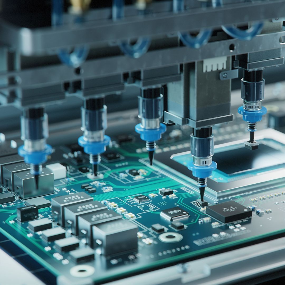
Modern electronic systems are built on printed circuit boards (PCBs), which offer a platform for connecting electrical parts. As electronic devices continue to operate at increasingly high speeds, it is essential to optimise the PCB design to minimise signal degradation, signal loss, and noise.
In this article, we will discuss some tips for optimising your PCB design for high-speed applications.
Ways to Optimise Printed Circuit Boards for High-Speed Applications
The methods for optimising your printed circuit boards for high-speed applications are listed below.
Select the Right PCB Material
The choice of PCB material has a significant impact on the performance of the board. High-speed applications require materials with low dielectric constants and low loss tangent values to minimise signal loss and maintain signal integrity. The choice of PCB material will depend on the specific application requirements and budget.
Minimise Signal Length
Signal length is a crucial factor that affects the performance of a high-speed PCB. The longer the signal path, the greater the chances of signal degradation, crosstalk, and electromagnetic interference (EMI). To minimise signal length, it is essential to use a multilayer PCB with a shorter trace length. The use of microstrip or stripline routing techniques can also help to reduce signal length.
Use Proper Grounding Techniques
Proper grounding is critical to maintaining signal integrity in high-speed PCBs. Ground planes should be placed adjacent to signal layers to reduce EMI and crosstalk. The ground planes should be connected to a single point, known as the star ground, to prevent ground loops. It is also essential to use bypass capacitors near the power supply pins to reduce noise.
Minimise Crosstalk
Crosstalk occurs when the signal on one trace interferes with the signal on another trace. This interference can lead to signal degradation and loss of data. To minimise crosstalk, it is essential to maintain proper spacing between the signal traces. The spacing between traces should be at least three times the trace width. The use of differential signalling can also help to reduce crosstalk.
Use Proper Termination Techniques
Termination is the process of properly matching the impedance of the transmission line to the load. Proper termination is critical to minimising signal reflections and maintaining signal integrity. The use of series and parallel termination techniques can help to match the impedance of the transmission line to the load.
Design for EMI/EMC
High-speed PCBs are susceptible to electromagnetic interference (EMI) and electromagnetic compatibility (EMC) issues. To minimise these issues, it is essential to design the PCB with EMI/EMC in mind. This can be achieved by using shielding techniques, grounding, and proper component placement.
Final Thoughts
In conclusion, optimising a PCB design for high-speed applications requires careful consideration of the materials used, signal length, grounding, crosstalk, termination, and EMI/EMC. By following these tips, you can minimise signal loss, signal degradation, and noise, leading to a more reliable and efficient electronic system. This is the best way to make sure your printed circuit boards are high-speed optimised.
M-Tek Assembly
At M-Tek Assembly we have decades of experience within the industry. We have achieved a
net-zero carbon footprint by using EVs, and for every printed circuit board we build, we plant a tree. Contact one of our SMT and PCB assembly experts today for assistance. Call
01189 455377 or follow us on
Twitter to learn more about our products and services.
Recent Posts